Laser-Patterned DEP Cell Trapping Chip
Active electrokinetic yeast cell trapping on transparent ITO glass microelectrodes without cleanroom lithography.
| Material | ITO coated glass, PMMA, transfer adhesive |
| Method | Direct laser ablation of ITO on glass, laser-cut PMMA channel, 25 µm transfer adhesive tape bonding, Pluronic F-127 surface passivation |
| Min feature | 50 µm castellated electrode gap |
| Idea to tested device | 4 days |
THE WORKFLOW
Cell isolation, dielectrophoretic (DEP) sorting, and bio-impedance measurements require planar microelectrodes embedded within fluidic channels. Typically, fabricating these structures requires expensive cleanroom photolithography, chrome masks, and thin-film metal evaporation, making iterative electrode optimization slow and costly.
HOW IT WAS BUILT
Castellated interdigitated electrode arrays patterned directly onto Indium Tin Oxide (ITO) coated glass slides via pulsed laser ablation. An optical PMMA fluidic channel is laser-cut and bonded to the substrate using a 25 µm transfer adhesive tape, with surface treatments applied to minimize non-specific cell adhesion.
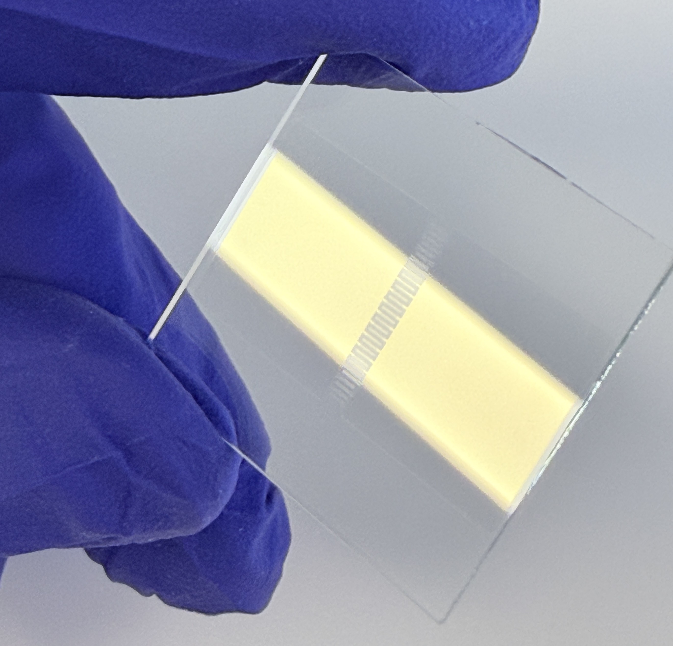 Detail of laser-ablated castellated ITO microelectrodes on glass, patterned directly without cleanroom photolithography.
BENCH CHARACTERIZATION
Verified with live yeast cell suspensions under 5 µL/min continuous hydrodynamic flow. When the AC voltage is activated, non-uniform electric field gradients reversibly trap cells along the castellated electrode tips. When the electric field is switched off, cells detach cleanly and resume laminar flow downstream without clogging the channel.
HOW THIS APPLIES TO YOUR DEVICE
If your instrument requires active cell manipulation, electrical impedance sensing, or electrowetting (EWOD), you do not need cleanroom chrome masks or thin-film evaporation to test feasibility. I can pattern custom transparent ITO electrode geometries (interdigitated, castellated, or quadrupole) directly on glass in hours, integrated into laser-cut PMMA or tape-laminated flow cells with anti-fouling surface treatments. You test working electrical hardware on your bench in days before committing to expensive silicon or glass foundry tooling.